LVDS PCB Layout Guidelines – Expert Tips for Clean Designs! Some lvds pcb layout guidelines for ensuring signal integrity
If you are looking for Some LVDS PCB Layout Guidelines for Ensuring Signal Integrity | PCB you've visit to the right page. We have 25 Pics about Some LVDS PCB Layout Guidelines for Ensuring Signal Integrity | PCB like LVDS: High Speed LVDS PCB Design Guidelines | MADPCB, FPGA - DAC LVDS 1.25GBPS PCB SKEW IMAGE - YouTube and also FPGA - DAC LVDS 1.25GBPS PCB SKEW IMAGE - YouTube. Read more:
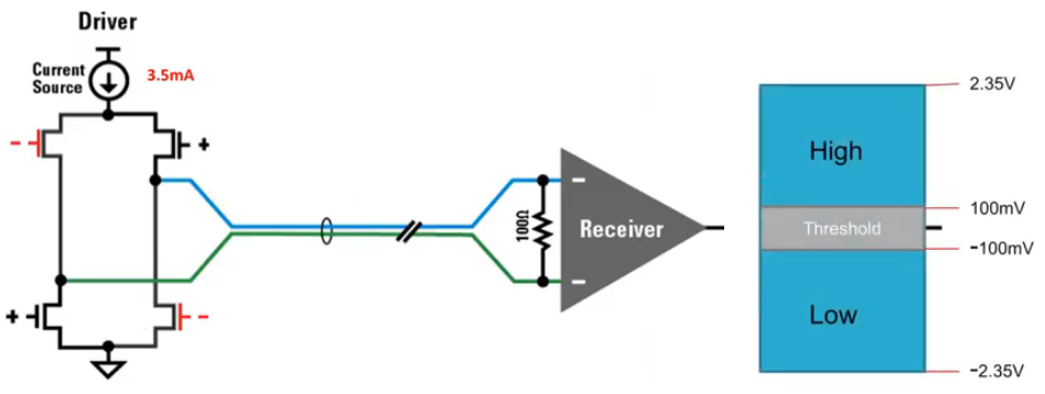
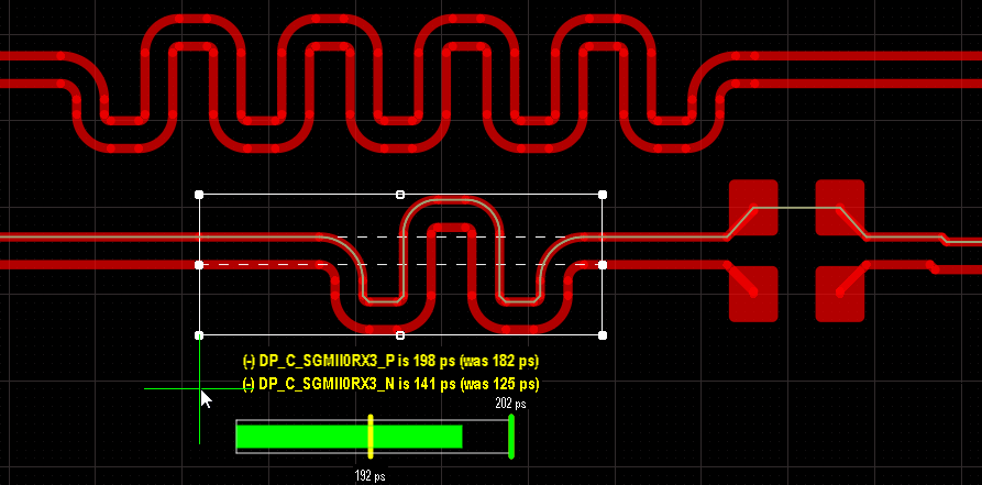
Some LVDS PCB Layout Guidelines For Ensuring Signal Integrity | PCB
 resources.altium.com
lvds pcb ensuring integrity altium buffer levels voltage physical
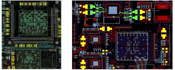
Main Design Guidelines & Layout Rules On High Speed PCB
 www.integrasources.com
Understanding LVDS Interface: A Comprehensive Guide
 www.shiningltd.com
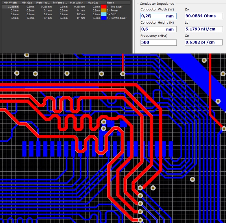
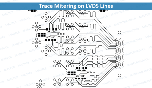
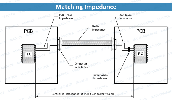
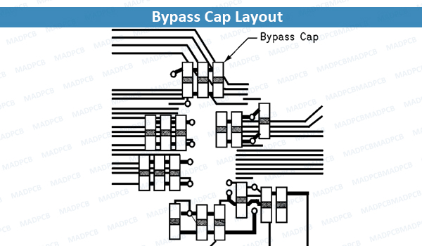
LVDS: High Speed LVDS PCB Design Guidelines | MADPCB
 madpcb.com
LVDS: High Speed LVDS PCB Design Guidelines | MADPCB
 madpcb.com
Some LVDS PCB Layout Guidelines For Ensuring Signal Integrity | PCB
FPGA - DAC LVDS 1.25GBPS PCB SKEW IMAGE - YouTube
 www.youtube.com
pcb lvds fpga skew
PCB Layout Guidelines For A Successful Design
 reversepcb.com
A Detailed Guide To PCB Layout Design – PCB HERO
 www.pcb-hero.com
An Ultimate Guide To Pcb Wiring And Layout - Vrogue.co
 www.vrogue.co
PCB Design Guidelines For High Current Applications - HardwareBee
 hardwarebee.com
pcb design layout guide high guidelines electronic ultimate process
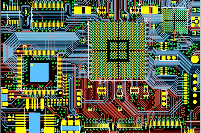
LVDS高速PCB布局布线设计_lvds等长差多少mil-CSDN博客
 blog.csdn.net
A Detailed Guide To PCB Layout Design - IBE Electronics
 www.pcbaaa.com
PCB Layout Support - Embizon Technologies - PCB Design Services, Bangalore
 www.embizon.com
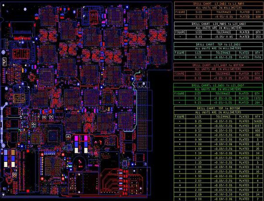
Pcb Layout Guidelines
 www.wellpcb.com
Some LVDS PCB Layout Guidelines For Ensuring Signal Integrity | PCB
Pcb Design & Layout, Your Expert For Pcb Design Service And Pcb Layout
 www.venture-mfg.com
PCB Design & PCB Layout : A Guide To Design The Right PCB
 www.hemeixinpcb.com
pcb layout
How To Design A PCB Layout: A Comprehensive Guide
 www.wevolver.com
Pcb Design Differential Impedance Of Lvds Rules And T - Vrogue.co
 www.vrogue.co
LVDS: High Speed LVDS PCB Design Guidelines | MADPCB
 madpcb.com
LVDS高速PCB布局布线设计_lvds等长差多少mil-CSDN博客
 blog.csdn.net
PCB Design Review: DPI-LVDS Sony Vaio LCD Devboard | Hackaday
 hackaday.com
Main Design Guidelines & Layout Rules On High Speed Printed Circuit
 www.integrasources.com
pcb gnd routing layout polygon ddr3 solid above crosstalk
Some LVDS PCB Layout Guidelines For Ensuring Signal Integrity | PCB
 resources.altium.com
Pcb layout guidelines. Some lvds pcb layout guidelines for ensuring signal integrity. Lvds: high speed lvds pcb design guidelines