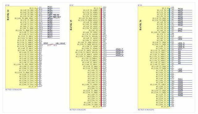
From Schematic to PCB: Step-by-Step Guide Even Beginners Can Follow! 10 steps to design a glx pcb main schematic
If you are searching about KiCAD 7 PCB Layout in 5 steps - YouTube you've came to the right web. We have 25 Pictures about KiCAD 7 PCB Layout in 5 steps - YouTube like How to Design a PCB Schematic: A Step-by-Step Guide, How to Convert Schematic Diagram into PCB layout? - Artist 3D and also 10 Steps to Design a GLX PCB Main Schematic. Here it is:
KiCAD 7 PCB Layout In 5 Steps - YouTube
 www.youtube.com
KiCAD 7 PCB Layout in 5 steps - YouTube
Guidelines For A Good Schematic Diagram Pcb Assemblypcb
 fity.club
Guidelines For A Good Schematic Diagram Pcb Assemblypcb
Guidelines For A Good Schematic Diagram Pcb Assemblypcb Printed Circuit
 fity.club
Guidelines For A Good Schematic Diagram Pcb Assemblypcb Printed Circuit ...
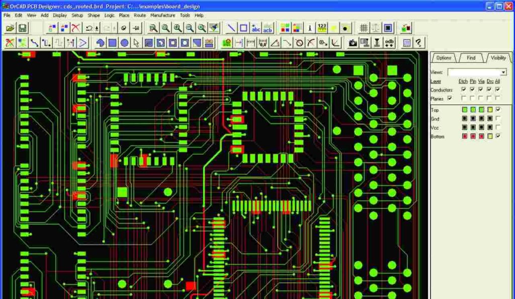
Step-by-step Cadence PCB Design Tutorial - RayPCB
 www.raypcb.com
Step-by-step cadence PCB design tutorial - RayPCB
How To Etch A PCB ? Step By Step - Artist 3D
 artist-3d.com
How to Etch a PCB ? Step by Step - Artist 3D
From Schematic Diagram To PCB Layout: Simplifying The Design Process
 elecschem.com
From Schematic Diagram to PCB Layout: Simplifying the Design Process
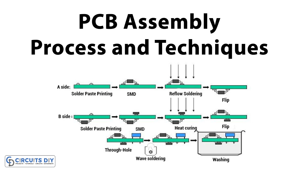
PCB Step-by-Step Guide How To Manufacture PCB Assembly And Fabrication
 www.pinterest.com
PCB Step-by-Step guide How to manufacture PCB Assembly and Fabrication ...
Pcb Layout Design Tutorial Pcb Design Steps & Complete Guide Maximizing
 pcblites.pages.dev
pcb layout design tutorial Pcb design steps & complete guide Maximizing ...
Pcb Designing How To Design A Pcb Step By Step – Artofit
 www.artofit.org
Pcb designing how to design a pcb step by step – Artofit
PCB Reverse Engineering: Comprehensive Guide For Beginners
 www.fscircuits.com
PCB Reverse Engineering: Comprehensive Guide for Beginners
How To Etch A PCB ? Step By Step - Artist 3D
 artist-3d.com
How to Etch a PCB ? Step by Step - Artist 3D
Step-by-step Cadence PCB Design Tutorial - RayMing PCB
 www.raypcb.com
Step-by-step cadence PCB design tutorial - RayMing PCB
PCB Manufacturing Process Distribution Guide-TechSparks
 www.tech-sparks.com
PCB Manufacturing Process Distribution Guide-TechSparks
Basic Steps To Design A PCB Layout – PCB HERO
 www.pcb-hero.com
Basic Steps to Design a PCB Layout – PCB HERO
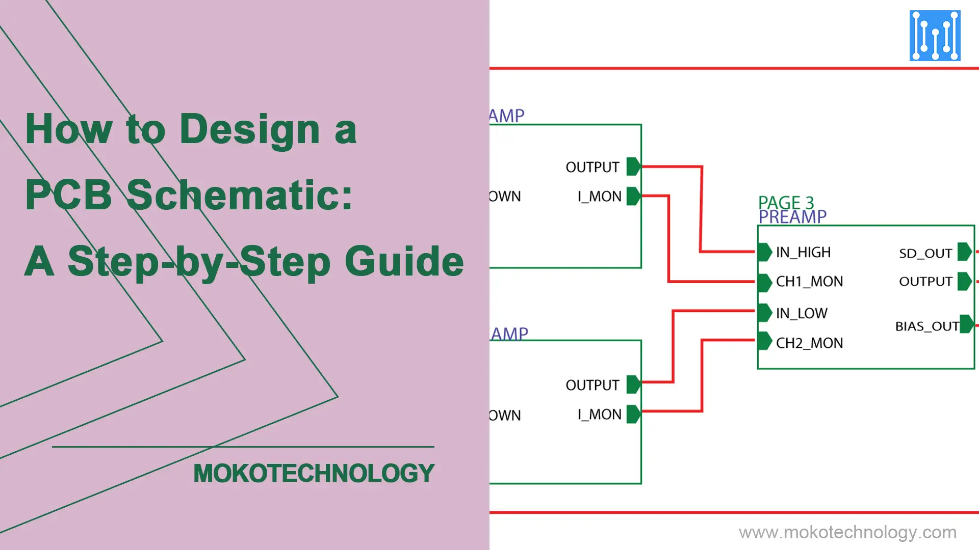
How To Design A PCB Schematic: A Step-by-Step Guide
 www.mokotechnology.com
How to Design a PCB Schematic: A Step-by-Step Guide
PCB-Herstellungsprozess | Schritt-für-Schritt-Anleitung Mit Flussdiagramm
 www.fs-pcba.com
PCB-Herstellungsprozess | Schritt-für-Schritt-Anleitung mit Flussdiagramm
PCB Designing: How To Design A PCB - Step By Step Guide
 www.electricaltechnology.org
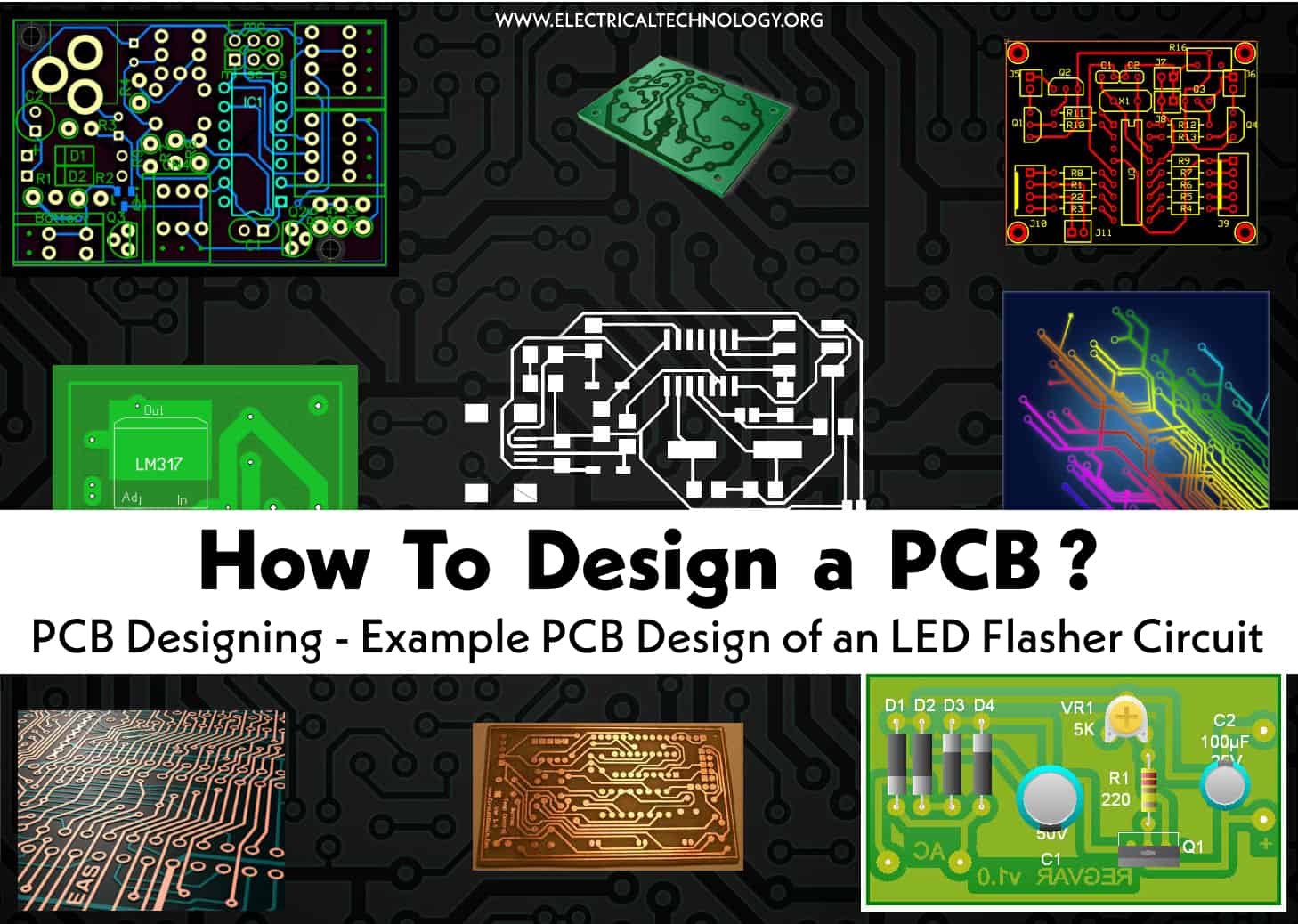
PCB Designing: How To Design a PCB - Step by Step Guide
Basics Of PCBs (What Is PCB, Types Of PCB, PCB Materials, 45% OFF
 www.alphamedicalmanagement.com
Basics Of PCBs (What Is PCB, Types Of PCB, PCB Materials, 45% OFF
PCB Layout Support - Embizon Technologies - PCB Design Services, Bangalore
 www.embizon.com
PCB Layout Support - Embizon Technologies - PCB Design Services, Bangalore
Step-by-Step Guide To PCB Design And Manufacturing - RayMing PCB
 www.raypcb.com
Step-by-Step Guide to PCB Design and Manufacturing - RayMing PCB
Beginner’s Guide To PCB Design: 10 Steps To Craft Your Own Printed
 creatiwise.com
Beginner’s Guide to PCB Design: 10 Steps to Craft Your Own Printed ...
10 Steps To Design A GLX PCB Main Schematic
 autoctrls.com
10 Steps to Design a GLX PCB Main Schematic
PCB Schematic Design – Step By Step Guide – PCB HERO
 www.pcb-hero.com
PCB Schematic Design – Step by Step Guide – PCB HERO
How To Convert Schematic Diagram Into PCB Layout? - Artist 3D
 artist-3d.com
How to Convert Schematic Diagram into PCB layout? - Artist 3D
Step-by-Step Guide To PCB Design And Manufacturing - RayMing PCB
 www.raypcb.com
Step-by-Step Guide to PCB Design and Manufacturing - RayMing PCB
step-by-step cadence pcb design tutorial. Pcb manufacturing process distribution guide-techsparks. from schematic diagram to pcb layout: simplifying the design process